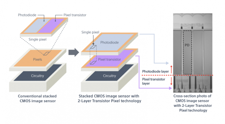
Sony’s Semiconductor Solutions Corporation has released a video that shows how their stacked CMOS image sensor technology with 2-Layer Transistor Pixel works. The technology can be found in Sony’s LYTIA smartphone sensors and it was first introduced in the Xperia 1 V.
This technology is said to prevent underexposure and overexposure in settings with a combination of bright and dim illumination (e.g., backlit settings) and enable high-quality, low-noise images even in low-light (e.g., indoor, nighttime) settings.
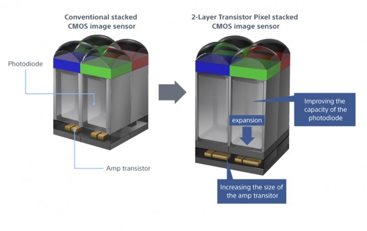
The 2-Layer Transistor pixel-stacked CMOS image sensor technology with a pixel structure separates photodiodes and pixel transistors on different substrate layers, as opposed to the conventional style of having the two on the same substrate. This new structure approximately doubles saturation signal level relative to conventional image sensors, widens dynamic range and reduces noise. This pixel structure will enable pixels to significantly improve their imaging properties even at smaller pixel sizes.