Panasonic claims they have developed the industry’s first 8K high-resolution, high-performance global shutter technology using an organic-photoconductive-film CMOS image sensor. The company says that the new technology enables 8K high resolution and high picture quality imaging without motion distortion, even when capturing extremely bright scenes.
The new 36MP sensor can capture up to 60fps in 8K resolution. It uses 450k high-saturation electrons and global shutter imaging with a sensitivity modulation function. The CMOS image sensor uses an organic photoconductive film (OPF). In this OPF CMOS image sensor, the photoelectric conversion part and the circuit are kept independent. By utilizing this OPF CMOS image sensor’s unique structure, Panasonic has been able to newly develop and incorporate high-speed noise cancellation technology and high saturation technology in the circuit part. By using this OPF CMOS image sensor’s unique sensitivity control function to vary the voltage applied to the OPF, Panasonic can provide a global shutter function. Panasonic claims that the technology that simultaneously achieves these performances is the industry’s first.
While this all sounds very technical, the sensor sounds like it is being made primarily with outside broadcast applications in mind where sports need to be captured in high frame rates, at high resolution, in contrasty conditions, where global shutter functionality is required to eliminate motion skew on fast moving objects. Panasonic also says that this sensor will work with a new electronically-controlled variable ND filter function which enables stepless adjustment of the OPF sensitivity by controlling the voltage applied to the OPF.
This new technology has the following benefits:
1. 8K resolution, 60fps frame rate, 450k saturation electrons and global shutter function can all be achieved simultaneously.
2. Switching between high sensitivity mode and high saturation mode is possible using a gain switching function.
3. The ND filter function can be used steplessly by controlling the voltage applied to the OPF.
Panasonic holds 135 Japanese patents and 83 overseas patents (including pending) related to this technology. The company presented some of these technologies at the international academic conference: ISSCC (International Solid-State Circuit Conference) 2018 which was held in San Francisco a week ago. If you want to know a bit more about how this technology works, you can read about it below, but it does get quite technical.
OPF CMOS image sensor design technology

The OPF CMOS image sensor has a unique structure, in which, the OPF performs a photoelectric conversion and the circuit area performs charge storage and signal readout functions completely independently. Using this OPF CMOS image sensor structure, Panasonic developed high-speed noise cancellation technology and high saturation technology in the circuit area which has a large available space. As a result, it is possible to simultaneously record an image in 8K resolution, with a 60fps framerate readout, with wide dynamic range (by achieving a high saturation level) and global shutter functionality.
In-pixel capacitive coupled noise cancellation technique

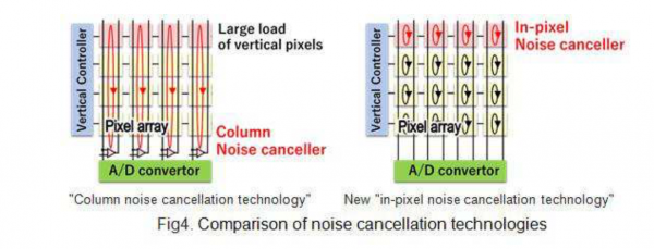
Because the OPF CMOS image sensor has a structure in which the OPF and the charge storage part are connected by metal plugs, accumulated charges cannot be completely read out. Therefore, there is a problem that it is affected by reset noise at the time of resetting the pixel (signal charge storage node). And, in a high-resolution sensor, such as an 8K sensor, it is necessary to drive large loads exceeding 4000 pixels aligned in the vertical direction at the same time as the time of noise cancellation, and therefore, the long time it takes to suppress noise is a problem. Panasonic developed a new structure that cancels pixel reset noise at high speed, even when high-resolution pixels have to be driven. In this structure, the reset noise is suppressed at high speed by using the negative feedback loop provided for each pixel.
In-pixel gain switching technology

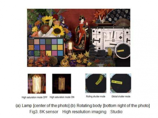
In the OPF CMOS image sensor, by incorporating a large capacitor in the circuit part with a large available area, it is possible to achieve both high sensitivity and high saturation with the same pixel structure merely by switching modes from the camera system. In the high sensitivity mode, it is possible to capture data up to a light intensity of 4.5k electrons with high sensitivity. Furthermore, by switching to the high saturation mode, it is possible to capture data up to a light intensity of 450k electrons. In this way, since the high saturation mode can capture up to 10 times the high sensitivity mode, it is possible to clearly display the fine winding structure of the lamp filaments, in which bright part gradation cannot be expressed, because it becomes overexposure in high sensitivity mode, as shown in the image above. Even in a scene with high contrast, it will be possible to capture brilliant images without overexposure or underexposure.
Voltage controlled sensitivity modulation technology
The OPF CMOS image sensor can change the sensitivity of the OPF simply by controlling the voltage applied to the OPF. By utilizing this function, Panasonic has been able to achieve the following functions which could not be done with conventional silicon image sensors.
Sensitivity Modulation Example 1: Global shutter function which can capture all pixels simultaneously at 8K resolution
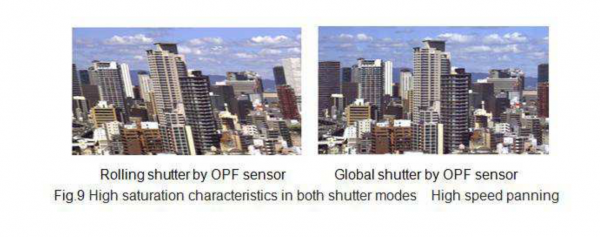
 By controlling ON / OFF of the voltage applied to the OPF and controlling the sensitivity of the OPF, Panasonic can provide a “global shutter function” capable of imaging all pixels at the same time, even driving a large number of pixels with an 8K sensor. By capturing with the global shutter function images can be read sharply without distortion. In a conventional global shutter type silicon image sensor, it is necessary to add new elements such as transfer circuits and charge storage capacitors in order to accumulate charges simultaneously in all pixels. As a result, the area of the photodiode and that of the additional circuits must compete for space, there is a problem that the pixel size cannot be reduced and the amount of saturation electrons cannot be increased. Conversely with an OPF CMOS image sensor, since there is no need for additional elements, it is possible to create small cell, high-resolution sensors, and by incorporating large capacitors in the circuit part with a large available area, accurate imaging with no distortion from dark scenes to extremely bright scenes is possible.
Sensitivity Modulation Example 2: “Electrical ND Filter Technology” which can change sensitivity continuously and without steps

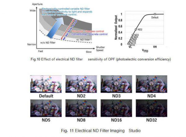
Conventionally it has been necessary to provide a plurality of ND filters according to conditions. With the OPF CMOS image sensor, by merely controlling the voltage applied to the OPF and changing the sensitivity of the OPF to the desired value, it is possible to electrically implement the ND filter function. This allows for continuous, step-less control of the sensitivity which could not be done with a conventional silicon sensor.
In the future, Panasonic plans to utilize this OPF CMOS image sensor technology in various applications such as broadcasting cameras, surveillance cameras, industrial inspection cameras, and automotive cameras etc.
I wouldn’t expect that we will see this new sensor appearing anytime soon in Panasonic’s digital cinema cameras, but it’s bound to find its way into outside broadcast cameras that will be used to cover the 2020 Tokyo Olympic games.


